6-Layer HDI Circuit Board Via in Pad PCB for GPS Tracking Applications
(Custom PCBs are tailored products; the images and specifications provided are for reference only.)
General Description
A 6-layer ultrathin printed circuit board (PCB) is built on an FR-4 substrate with a Tg of 135°C, specifically designed for GPS tracking applications. With a thickness of just 0.6 mm, the PCB features a green solder mask (Taiyo) and immersion gold on the pads, without any silkscreen. The base material is sourced from Taiwan's ITEQ, providing one PCB per panel. The vias, measuring 0.25 mm, are resin-filled and capped (via in pad), with blind vias extending from the top layer to inner layer 1 and buried vias connecting inner layer 3 to inner layer 4. Fabrication complies with IPC 6012 Class 2 standards using supplied Gerber data, and each shipment contains 50 panels.
Features and Benefits
Via in Pad Design: Reduces inductive and capacitive reactance in transmission lines.
Immersion Gold Finish: Ensures high solderability, minimizes stress on circuit boards, and reduces surface contamination.
Certified Manufacturing: Products are certified by authorized organizations.
High First Production Rate: Over 95% of products meet quality standards on the first production run.
Scalable Production: Capable of transitioning from prototype to volume production.
Timely Delivery: Achieves over 98% on-time delivery rate.
Expertise: More than 18 years of experience in PCB manufacturing.
IPC Compliance: Manufactured to IPC Class 2 and Class 3 standards.
.jpg)
PCB Specifications
| PCB SIZE | 100 x 103mm=1PCS |
| BOARD TYPE | Multilayer PCB |
| Number of Layers | 6 layers |
| Surface Mount Components | YES |
| Through Hole Components | NO |
| LAYER STACKUP | copper ------- 18um(0.5oz)+plate TOP CS |
| 4mil prepreg | |
| copper ------- 18um(0.5oz) GND Plane | |
| 4mil FR-4 | |
| copper ------- 18um(0.5oz) PWR Plane | |
| 4mil prepreg | |
| copper ------- 18um(0.5oz) PWR Plane | |
| 4mil FR-4 | |
| copper ------- 18um(0.5oz) SIG | |
| 4mil prepreg | |
| copper ------- 18um(0.5oz) BOT PS | |
| TECHNOLOGY | |
| Minimum Trace and Space: | 3mil/3mil |
| Minimum / Maximum Holes: | 0.22/3.50mm |
| Number of Different Holes: | 25 |
| Number of Drill Holes: | 2315 |
| Number of Milled Slots: | 0 |
| Number of Internal Cutouts: | 0 |
| Impedance Control | no |
| BOARD MATERIAL | |
| Glass Epoxy: | FR-4, ITEQ IT140 TG>135, er<5.4 |
| Final foil external: | 1oz |
| Final foil internal: | 0.5oz |
| Final height of PCB: | 0.6mm ±0.1 |
| PLATING AND COATING | |
| Surface Finish | Immersion gold 0.025µm over 3µm Nickel (14.4% area) |
| Solder Mask Apply To: | TOP and Bottom, 12micron Minimum |
| Solder Mask Color: | Green, TAIYO PSR-2000 GT600D |
| Solder Mask Type: | LPSM |
| CONTOUR/CUTTING | Routing |
| MARKING | |
| Side of Component Legend | No silkscreen requried. |
| Colour of Component Legend | No silkscreen requried. |
| Manufacturer Name or Logo: | No silkscreen requried. |
| VIA | Plated through hole(PTH), Blind via and via capping on CS and PS, vias not be visible. |
| FLAMIBILITY RATING | UL 94-V0 Approval MIN. |
| DIMENSION TOLERANCE | |
| Outline dimension: | 0.0059" (0.15mm) |
| Board plating: | 0.0030" (0.076mm) |
| Drill tolerance: | 0.002" (0.05mm) |
| TEST | 100% Electrical Test prior shipment |
| TYPE OF ARTWORK TO BE SUPPLIED | email file, Gerber RS-274-X, PCBDOC etc |
| SERVICE AREA | Worldwide, Globally. |
.jpg)
Typical Applications
LED Lighting
Intercom Systems
Portable WiFi Routers
GSM Trackers
Commercial LED Lighting
4G WiFi Modems
Honeywell Access Control
Electronic Access Control Systems
Audio Frequency Amplifiers
File Servers
.jpg)
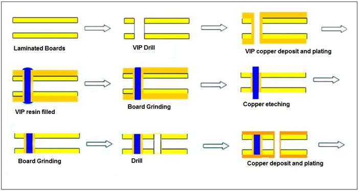
Via in Pad Technology
As circuit boards become denser and more interconnected, the need for efficient routing has led to the development of via in pad technology. This method involves plating through holes that are filled with insulating resin, followed by drying, grinding, and electroplating. As a result, the entire surface of the PCB is coated with copper, eliminating visible via holes.
The benefits of via in pad technology include improved electrical performance and reliability, shortened signal transmission paths, reduced inductive and capacitive reactance, and minimized electromagnetic interference.
Basic Process of Via in Pad
Drilling and Filling: Holes are drilled and filled with insulating resin.
Drying and Grinding: The surface is dried and ground to a smooth finish.
Electroplating: The entire surface receives a copper coating, enhancing conductivity.
This innovative approach is essential for modern high-performance electronic products.